

Product Code : ST-Si-5N-Cu
N-type Silicon (Si) sputtering target is a type of thin-film deposition material used for the fabrication of electronic components such as solar cells, semiconductor devices, and integrated circuits. Sputtering targets are typically made from high-purity materials and are used to deposit thin films of the substrate material onto a substrate surface through a technique called sputtering.
N-type Silicon (Si) targets are a type of silicon sputtering target doped with impurities such as phosphorus, arsenic, or antimony to create a material with excess electrons, resulting in a high conductivity (low resistivity) material. This makes it a critical material for the fabrication of electronic devices where electrical conductivity is important, such as transistors, diodes, and solar cells.
The manufacturing process of N-type Silicon (Si) sputtering target involves melting the high-purity silicon material with the desired impurities in an induction furnace to create uniformity. This is followed by solidification into a pre-defined shape, typically as a disc, and polishing to a high degree of surface quality.
The N-type Silicon (Si) sputtering targets vary in thickness and size depending on the specific use and application. They are commonly used for deposition through techniques such as radio frequency (RF) magnetron sputtering, direct current (DC) sputtering, and pulsed laser deposition (PLD) to create thin films of high-purity, high-conductivity N-type Silicon (Si) for a range of electronic applications.
Please contact us if you need customized services. We will contact you with the price and availability in 24 hours.
| Product | Product Code | Purity | Size | Contact Us |
Product Information
N-type Silicon (Si) sputtering target is a type of thin-film deposition material used for the fabrication of electronic components such as solar cells, semiconductor devices, and integrated circuits. Sputtering targets are typically made from high-purity materials and are used to deposit thin films of the substrate material onto a substrate surface through a technique called sputtering.
N-type Silicon (Si) targets are a type of silicon sputtering target doped with impurities such as phosphorus, arsenic, or antimony to create a material with excess electrons, resulting in a high conductivity (low resistivity) material. This makes it a critical material for the fabrication of electronic devices where electrical conductivity is important, such as transistors, diodes, and solar cells.
The manufacturing process of N-type Silicon (Si) sputtering target involves melting the high-purity silicon material with the desired impurities in an induction furnace to create uniformity. This is followed by solidification into a pre-defined shape, typically as a disc, and polishing to a high degree of surface quality.
The N-type Silicon (Si) sputtering targets vary in thickness and size depending on the specific use and application. They are commonly used for deposition through techniques such as radio frequency (RF) magnetron sputtering, direct current (DC) sputtering, and pulsed laser deposition (PLD) to create thin films of high-purity, high-conductivity N-type Silicon (Si) for a range of electronic applications.
Chemical Formula:Si
Synonyms
N/A
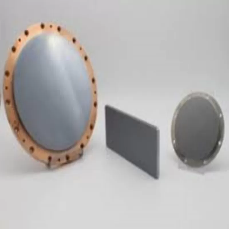
N-type Silicon (Si) Sputtering Target Specification
Shape: Disc/Rectangular/Tube
Bonding: Unbonding/Bonding
Per your request or drawing
We can customized as required
Size:
| Circular Sputtering Targets | Diameter | 1.0”2.0”3.0”4.0”5.0”6.0”up to 21” |
| Rectangular Sputtering Targets | Width x Length | 5” x 12”5” x 15”5” x 20”5” x 22”6” x 20” |
| Thickness | 0.125”, 0.25” | |
Sputtering Targets Requirements
General requirements such as size, flatness, purity, impurity content, density, N/O/C/S, grain size, and defect control. Special requirements include surface roughness, resistance value, grain size uniformity, composition and tissue uniformity, magnetic conductivity, ultra-high density, ultra-fine grains, etc.
Application of N-type Silicon (Si) Sputtering Target
N-type Silicon (Si) Sputtering Target is mainly used in the electronics and information industry, glass coating field, wear-resistant materials, high-temperature corrosion resistance, high-grade decorative goods, and other industries.
Packing of N-type Silicon (Si) Sputtering Target
Standard Packing:
Typical bulk packaging includes palletized plastic 5 gallon/25 kg. pails, fiber and steel drums to 1 ton super sacks in full container (FCL) or truck load (T/L) quantities. Research and sample quantities and hygroscopic, oxidizing or other air sensitive materials may be packaged under argon or vacuum. Solutions are packaged in polypropylene, plastic or glass jars up to palletized 440 gallon liquid totes Special package is available on request.
ATTs’N-type Silicon (Si) Sputtering Target is carefully handled to minimize damage during storage and transportation and to preserve the quality of our products in their original condition.
")
 Sputtering Target")
 Sputtering Target")
