Product Code : EM-AI2O3-NN-CU1
Sapphire is a material of a unique combination of physical, chemical and optical properties, which make it resistant to high temperature, thermal shock, water and sand erosion, and scratching. Comparing to other wafers, the sapphire wafer has many unique features such as high strength, anti-corrosion, anti-abrasion, good thermal conductivity, and good electrical isolation.
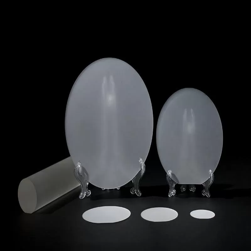
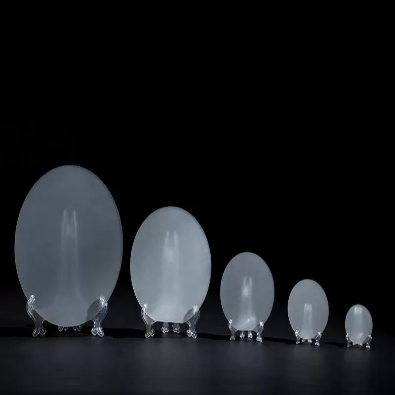
ATT manufactures high purity single crystal Sapphire Wafers for optoelectronics applications. Our standard wafer diameters range from 25.4 mm (1 inch) to 300 mm (11.8 inches) in size; wafers can be produced in various thicknesses and orientations with polished or unpolished sides and can include dopants. We can offer complete orientation options including C plane, A plane, R plane and M plane.
Please contact us if you need customized services. We will contact you with the price and availability in 24 hours.
| Product | Product Code | Purity | Size | Contact Us |
Product Information
Sapphire is a material of a unique combination of physical, chemical and optical properties, which make it resistant to high temperature, thermal shock, water and sand erosion, and scratching. Comparing to other wafers, the sapphire wafer has many unique features such as high strength, anti-corrosion, anti-abrasion, good thermal conductivity, and good electrical isolation. Due to its excellent mechanical and chemical characteristics, the sapphire wafer plays an important role in the optoelectronics industry and widely used in precision mechanical parts and vacuum equipment. It is a superior window material for many IR applications from 3µm to 5µm. C-plane sapphire substrates are widely used to grow III-V and II-VI compounds such as GaN for blue LED and laser diodes, while R-plane sapphire substrates are used for the hetero-epitaxial deposition of silicon for microelectronic IC applications.
ATT manufactures high purity single crystal Sapphire Wafers for optoelectronics applications. Our standard wafer diameters range from 25.4 mm (1 inch) to 300 mm (11.8 inches) in size; wafers can be produced in various thicknesses and orientations with polished or unpolished sides and can include dopants. We can offer complete orientation options including C plane, A plane, R plane and M plane.
Synonyms
Alumina; aluminium oxide; aluminum(III) oxide; aluminium(III) oxide; aloxide; aloxite; alundum; oxo-oxoalumanyloxy-alumane, sapphire; corundum; aluminum trioxide; alumina ceramic; alpha-Corundum; bauxite; Electrocorundum; keto-ketoalumanyloxy-alumane
Sapphire Wafer Specification
| Orientation | R-plane, C-plane, A-plane, M-plane or a specified orientation |
| Orientation Tolerance | ± 0.3° |
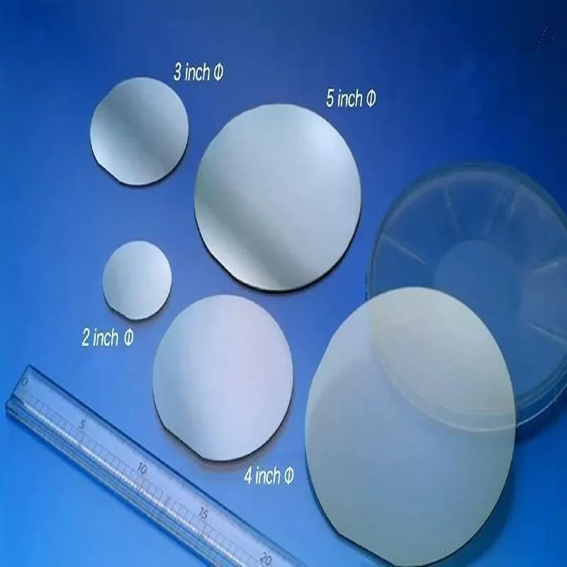
| Diameter | 2 inches, 3 inches, 4 inches, 6 inches, 8 inches or others |
| Diameter Tolerance | 0.1mm for 2 inches, 0.2mm for 3 inches, 0.3mm for 4 inches, 0.5mm for 6 inches |
| Thickness | 0.25mm, 0.33mm, 0.43mm, 0.65mm, 1mm or others; |
| Thickness Tolerance | 25μm |
| Primary Flat Length | 16.0±1.0mm for 2 inches, 22.0±1.0mm for 3 inches, 30.0±1.5mm for 4 inches, 47.5/50.0±2.0mm for 6 inches |
| Primary Flat Orientation | A-plane (1 1-2 0 ) ± 0.2°; C-plane (0 0-0 1 ) ± 0.2°, Projected C-Axis 45 +/- 2° |
| TTV | ≤10µm for 2 inches, ≤15µm for 3 inches, ≤20µm for 4 inches, ≤25µm for 6 inches |
| BOW | ≤10µm for 2 inches, ≤15µm for 3 inches, ≤20µm for 4 inches, ≤25µm for 6 inches |
| Front Surface | Epi-Polished (Ra< 0.3nm for C-plane, 0.5nm for other orientations) |
| Back Surface | Fine ground (Ra=0.6μm~1.4μm) or Epi-polished |
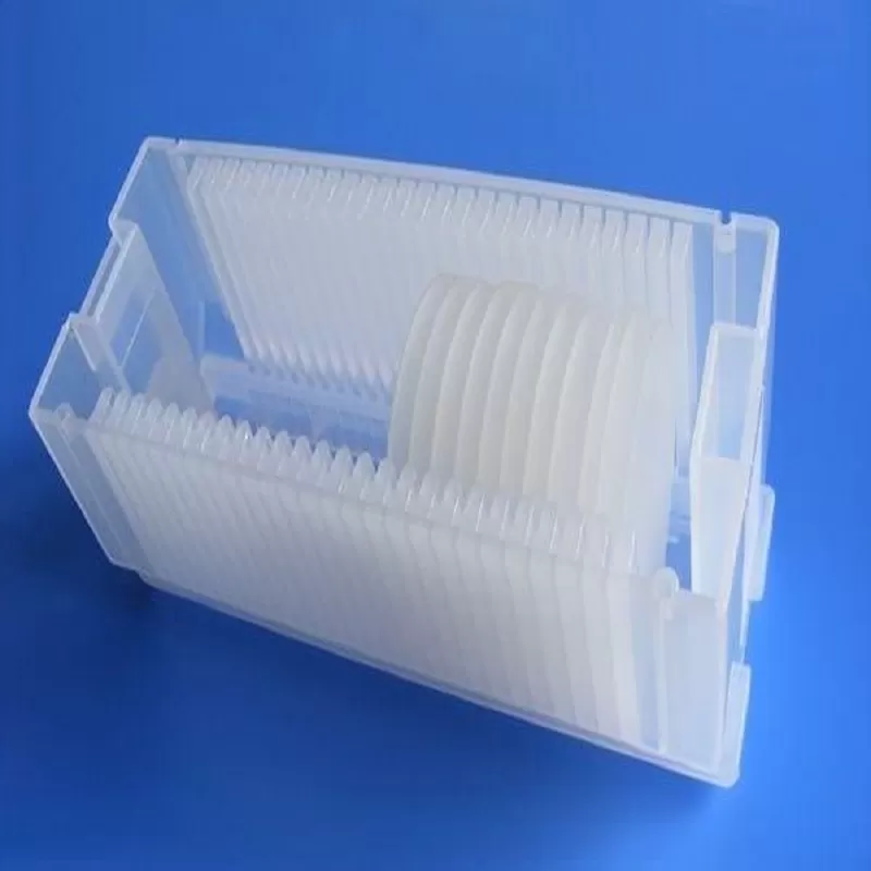
| Packaging | Packaged in a class 100 clean room environment |
Per your request or drawing
We can customized as required
Properties(Theoretical)
| Compound Formula | Al2O3 |
| Molecular Weight | 101.96 |
| Appearance | Wafer |
| Melting Point | 2050 °C (3720 °F) |
| Boiling Point | 2,977° C (5,391° F) |
| Density | 4.0 g/cm3 |
| Refractive Index | 1.8 |
| Electrical Resistivity | 17 10x Ω-m |
| Poisson's Ratio | 0.28 |
| Specific Heat | 760 J Kg-1 K-1 (293K) |
| Tensile Strength | 1390 MPa (Ultimate) |
| Thermal Conductivity | 30 W/m-K |
| Thermal Expansion | 5.3 µm/m-K |
| Young's Modulus | 450 GPa |
| Exact Mass | 101.948 g/mol |
| Monoisotopic Mass | 101.94782 Da |
Applications of Sapphire Wafer
High-frequency device
High power device
GaN epitaxy device
High-temperature device
Optoelectronic device
Light-emitting diode
Growth substrate for III-V and II-VI compounds
Electronics and optoelectronics
IR applications
Silicon On Sapphire Integrated Circuit(SOS)
Radio Frequency Integrated Circuit(RFIC)
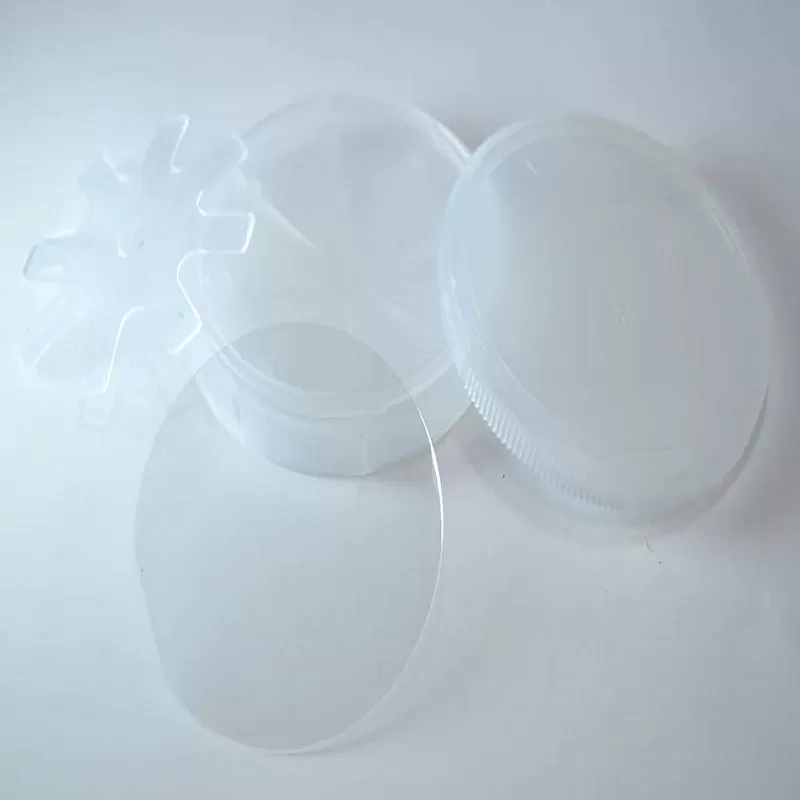
Packing of Sapphire Wafer
Standard Packing:
Typical bulk packaging includes palletized plastic 5 gallon/25 kg. pails, fiber and steel drums to 1 ton super sacks in full container (FCL) or truck load (T/L) quantities. Research and sample quantities and hygroscopic, oxidizing or other air sensitive materials may be packaged under argon or vacuum. Solutions are packaged in polypropylene, plastic or glass jars up to palletized 440 gallon liquid totes Special package is available on request.
ATTs’ Sapphire Wafer is carefully handled to minimize damage during storage and transportation and to preserve the quality of our products in their original condition.
Chemical Identifiers
| Linear Formula | Al2O3 |
| CAS #: | 1344-28-1 |
| MDL Number | MFCD00003424 |
| EC No. | N/A |
| Beilstein/Reaxys No. | N/A |
| Pubchem CID | 14769 |
| IUPAC Name | Oxo(oxoalumanyloxy)alumane |
| SMILES | O=[Al]O[Al]=O |
| InchI Identifier | InChI=1S/2Al.3O |
| InchI Key | TWNQGVIAIRXVLR-UHFFFAOYSA-N |