Product Code : EM-SiC-NN-CU1
As a next-generation semiconductor material, silicon carbide wafer has unique electrical properties and excellent thermal properties. Due to Silicon Carbide (SiC) physical and electronic properties, SiC based devices are well suitable for short wavelength optoelectronic, high temperature, radiation resistant, and high-power/high-frequency electronic devices, compared with Si and GaAs based devices.
We offer 6H and 4H N type conductive SiC substrates and 6H and 4H semi-insulating SiC substrates in different quality grades. Micro-pipe density of less than 2 per cm2 is available upon request. The sic-based device has been used for short-wavelength optoelectronic, high temperature, radiation resistant applications. In the applications of high power and high temperature, SiC wafer is more suitable compared to the silicon wafer and GaAs wafer.
wafers can be produced in various thicknesses and orientations with polished or unpolished sides and can include dopants.
ATT offers the best price on the market for high quality SiC wafers and SiC crystal substrates,SiC Epitaxy up to six (6) inch diameter. Both N-Type and Semi-Insulating Type 4H 6 inch SiC wafers are available.
Please contact us if you need customized services. We will contact you with the price and availability in 24 hours.
| Product | Product Code | Purity | Size | Contact Us |
Product Information
As a next-generation semiconductor material, silicon carbide wafer has unique electrical properties and excellent thermal properties. Due to Silicon Carbide (SiC) physical and electronic properties, SiC based devices are well suitable for short wavelength optoelectronic, high temperature, radiation resistant, and high-power/high-frequency electronic devices, compared with Si and GaAs based devices.
SiC Epitaxy:
We provide custom thin film SiC epitaxy on 6H or 4H substrates for the development of silicon carbide devices. SiC epi wafer is mainly used for Schottky diodes, metal-oxide semiconductor field-effect transistors, junction field effect transistors, bipolar junction transistors, insulated gate bipolar as well as other applications.
SiC conductive substrates and SiC semi-insulating substrates:
We offer 6H and 4H N type conductive SiC substrates and 6H and 4H semi-insulating SiC substrates in different quality grades. Micro-pipe density of less than 2 per cm2 is available upon request. The sic-based device has been used for short-wavelength optoelectronic, high temperature, radiation resistant applications. In the applications of high power and high temperature, SiC wafer is more suitable compared to the silicon wafer and GaAs wafer.
wafers can be produced in various thicknesses and orientations with polished or unpolished sides and can include dopants.
ATT offers the best price on the market for high quality SiC wafers and SiC crystal substrates,SiC Epitaxy up to six (6) inch diameter. Both N-Type and Semi-Insulating Type 4H 6 inch SiC wafers are available.
Synonyms
methanidylidynesilicon; Carborundum; Silicon monocarbide; Betarundum Carborundeum; carbon silicide; Green densic
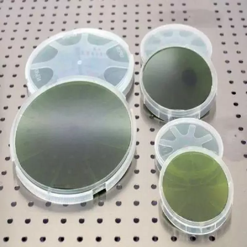
Silicon Carbide Wafer Specification
Diameter:2 inches, 3 inches, 4 inches, 6 inches or others
| Grade | Zero MPD Grade | Production Grade | Research Grade | Dummy Grade | |
| Diameter | 150.0 mm +/- 0.2 mm | ||||
| Thickness | 500 um +/- 25 um for 4H-SI350 um +/- 25 um for 4H-N | ||||
| Wafer Orientation | On axis: <0001> +/- 0.5 deg for 4H-SIOff axis: 4.0 deg toward <11-20> +/-0.5 deg for 4H-N | ||||
| Micropipe Density (MPD) | 1 cm-2 | 5 cm-2 | 15 cm-2 | 30 cm-2 | |
| Electrical Resistivity(Ohm-cm) | 4H-N | 0.015~0.025 | |||
| 4H-SI | >1E5 | (90%) >1E5 | |||
| Doping Concentration | N-type: ~ 1E18/cm3SI-type (V-doped): ~ 5E18/cm3 | ||||
| Primary Flat (N type) | {10-10} +/- 5.0 deg | ||||
| Primary Flat Length (N type) | 47.5 mm +/- 2.0 mm | ||||
| Notch (Semi-Insulating type) | Notch | ||||
| Edge exclusion | 3 mm | ||||
| TTV /Bow /Warp | 15um /40um /60um | ||||
| Surface Roughness | Polish Ra 1 nm | ||||
| CMP Ra 0.5 nm on the Si face | |||||
| Cracks by high intensity light | None | None | 1 allowed, 2 mm | Cumulative length 10 mm, single length 2 mm | |
| Hex Plates by high intensity light* | Cumulative area 0.05 % | Cumulative area 0.05 % | Cumulative area 0.05 % | Cumulative area 0.1 % | |
| Polytype Areas by high intensity light* | None | None | Cumulative area 2% | Cumulative area 5% | |
| Scratches by high intensity light** | 3 scratches to 1 x wafer diameter cumulative length | 3 scratches to 1 x wafer diameter cumulative length | 5 scratches to 1 x wafer diameter cumulative length | 5 scratches to 1 x wafer diameter cumulative length | |
| Edge chip | None | 3 allowed, 0.5 mm each | 5 allowed, 1 mm each | ||
| Contamination by high intensity light | None | ||||
Notes: * Defect limits are applicable to the entire wafer surface except for the edge exclusion area, where defects are present. ** The scratches are checked on the Si face only.
Properties Of 4H Silicon Carbide Crystal Material
| Property | 4H-SiC Single Crystal |
| Lattice Parameters (Å) | a=3.076c=10.053 |
| Stacking Sequence | ABCB |
| Density | 3.21 |
| Mohs Hardness | ~9.2 |
| Thermal Expansion Coefficient (CTE) (/K) | 4-5 x 10⁻⁶ |
| Refraction Index @750nm | no = 2.61ne = 2.66 |
| Dielectric Constant | c ~ 9.66 |
| Doping Type | N-type or Semi-insulating |
| Thermal Conductivity (W/cm-K @298K)(N-type, 0.02 ohm-cm) | a~4.2c~3.7 |
| Thermal Conductivity (W/cm-K @298K)(Semi-insulating type) | a~4.9c~3.9 |
| Band-gap (eV) | 3.23 |
| Break-Down Electrical Field (V/cm) | 3-5 x 10⁶ |
| Saturation Drift Velocity (m/s) | 2.0 x 10⁵ |
| Wafer and Substrate Sizes | Wafers: 2, 3, 4, 6 inch; smaller substrates: 10x10, 20x20 mm, other sizes are available and can be custom-made upon request |
| Product Grades | A Grade Zero micropipe density (MPD < 1 cm-2)B Grade Production grade (MPD < 5 cm-2)C Grade Research grade (MPD < 15 cm-2)D Grade Dummy grade (MPD < 30 cm-2) |
Silicon Carbide Material Properties:
| Materials | Single Crystal 6H | Single Crystal 4H |
| Lattice Parameters | a=3.073 Å, c=15.117 Å | a=3.076 Å , c=10.053 Å |
| Stacking Sequence | ABCACB | ABCB |
| Band-gap | 3.02 eV | 3.27 eV |
| Density | 3.21 g/cm3 | 3.21 g/cm3 |
| Therm. Expansion Coefficient | 4~5×10⁻⁶/K | 4~5×10⁻⁶/K |
| Refraction Index | no = 2.707, ne = 2.755 | no = 2.719, ne = 2.777 |
| Dielectric Constant | 9.66 | 9.6 |
| Thermal Conductivity | 490 W/m·K | 490 W/m·K |
| Break-Down Electrical Field | 2 ~ 4 · 108 V/m | 2 ~ 4 · 108 V/m |
| Saturation Drift Velocity | 2.0 · 105 m/s | 2.0 · 105 m/s |
| Electron Mobility | 400 cm2/V·S | 800 cm2/V·S |
| hole Mobility | 90 cm2/V·S | 115 cm2/V·S |
| Mohs Hardness | ~ 9 | ~ 9 |
Applications of Silicon Carbide Wafers
High-frequency device
High power device
GaN epitaxy device
High-temperature device
Optoelectronic device
Light-emitting diode
Packing of Silicon Carbide Wafers
Standard Packing:
Typical bulk packaging includes palletized plastic 5 gallon/25 kg. pails, fiber and steel drums to 1 ton super sacks in full container (FCL) or truck load (T/L) quantities. Research and sample quantities and hygroscopic, oxidizing or other air sensitive materials may be packaged under argon or vacuum. Solutions are packaged in polypropylene, plastic or glass jars up to palletized 440 gallon liquid totes Special package is available on request.
ATTs’ Silicon Carbide Wafers is carefully handled to minimize damage during storage and transportation and to preserve the quality of our products in their original condition.
Chemical Identifiers
| Linear Formula | SiC |
| CAS #: | 409-21-2 |
| MDL Number | MFCD00049531 |
| EC No. | 206-991-8 |
| Beilstein/Reaxys No. | N/A |
| Pubchem CID | 9863 |
| IUPAC Name | methanidylidynesilicon |
| SMILES | [C-]#[Si+] |
| InchI Identifier | InChI=1S /CSi/c1-2 |
| InchI Key | HBMJWWWQQXIZIP-UHFFFAOYSA-N |